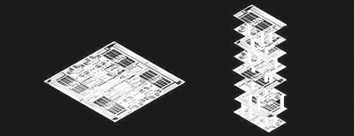
For decades, "smaller, faster and cheaper" has become the curse for the development of electronic devices. Recently, engineers at Stanford University in the United States added a fourth—higher. At the Institute of Electrical and Electronics Engineers (IEEE) International Electronic Equipment Conference held in San Francisco, USA, from December 15th to 17th, the Stanford University research team introduced how to build a "multi-layer" chip that can greatly increase the current level of circuit card billing. Layer logic and memory chip performance. Four-layer "multi-layer chip" prototype developed by Stanford University engineers. The bottom and top layers are logic transistors, and the middle layer is two layers of memory chips. Vertical tubes are nanoscale electronic "elevators" that connect the logic and storage layers so that they work together to solve problems. On the left is the current single-layer circuit card. The logic and memory chips are separated in different areas and connected by wires. Just like city streets, congestion often occurs because data is transmitted back and forth between logical areas and storage areas. On the right is a multi-layered logic chip and memory chip, forming a "skyscraper" type chip. The data is transmitted through the nano "elevator" to achieve three-dimensional transmission, avoiding congestion. A circuit card is like a busy city, storing data on a memory chip and calculating it through a logic chip. When the computer is busy, "digital traffic jams" occur on the lines connecting the logic chip and the memory chip, and the "multilayer" chip can end this congestion. This new solution can superimpose logic layers on the storage layer, tightly and interconnected, and transport data between layers through thousands of nano-electronic “lifts†that will connect the current single-layer logic chips and memory chips. Faster line speeds and less power consumption. Three breakthroughs The study was led by Sambosis Mithra, a professor of electrical engineering and computer science at Stanford University, and HS Philip Weng. According to the research team, their innovation research has achieved three breakthroughs: The first is the new technology for manufacturing transistors, the transistors are tiny gates, which represent 1 and 0 by switching current, and the second is a new type of computer memory with multiple layers. Structure; The third is to integrate the new technology of manufacturing logic gates and memory into a new technology of multi-layer structure, which is completely different from the previous stacking chips. "This research is still in the early stages, but our design and manufacturing technology is scalable," Mitra said. "With future developments, this structure will greatly increase the performance of computers beyond any existing computer." ." Weng said that the prototype of this chip has been exhibited at last year's International Electronic Devices Conference (IEDM), showing how logic and memory chips can be combined into a three-dimensional structure that can be mass-produced. It can be said that this changed the chip's paradigm. "With this new structure, electronics manufacturing will turn your computer into a powerful supercomputer." Carbon nanotube fabrication logic layer Engineers have built silicon chips decades ago. However, whether the mobile phone or the tablet PC is hot, the size of the emitted heat can also show its internal problems. Even if they are closed, sometimes there is leakage of electricity from the silicon transistors. The user will feel hot, and the system itself, this leak will also run out of battery, wasting power. Researchers are working to solve this problem, such as using carbon nanotube (CNT) transistors. Carbon nanotubes are very thin, and 2 billion roots have a hair thickness, so the leakage is much less than silicon. In the second conference paper of Mitra and Weng, they described how they made the highest performance carbon nanotube transistors. With the standard process of producing carbon nanotubes in the past, the densities of nanotubes produced were not dense enough. They have overcome this problem and developed a flexible technology that can pack enough carbon nanotubes in a small enough area to make a useful chip. They first used standard methods to produce carbon nanotubes on a round quartz wafer, and then increased the thickness to a certain amount. Then the entire carbon nanotube layer was peeled off from the quartz medium and deposited on the silicon wafer. This silicon wafer is the basis of their multilayer chip. Researchers must first fabricate carbon nanotube layers with sufficient density to produce high-performance logic devices. They repeated this process 13 times, growing a large number of carbon nanotubes on a quartz wafer, and then stripping them using a transfer technique to deposit them on a silicon wafer. Using this simple technology to fix, they created some of the highest density and highest performance carbon nanotubes ever. They also proved that this technology can be implemented in more than one logical layer when manufacturing multi-layer chips. "Sandwich" memory Creating a high-performance CNT transistor layer is only part of a multi-layer chip. It is equally important to make a memory chip directly on each CNT transistor layer. Weng is the leader in manufacturing this type of memory. Weng designed a new type of memory that is completely different from the current memory. Instead of silicon, it uses titanium nitride, germanium dioxide, and platinum to form a metal-oxide-metal sandwich structure that can be energized in one direction. Resistors, which conduct electricity in the opposite direction. The change from the resistance to the conductive state is the way the new memory technology forms the digits 0 and 1, so its name is called Resistive Random Access Memory or RRAM. RRAM consumes less power than current memory and can be used on mobile devices to extend battery life. This new storage technology is also key to manufacturing multilayer chips because RRAM can be manufactured at lower temperatures than silicon memory. Multilayer interconnection The conference demonstrated four-layer chips made by Max Schleuck and Tony Wu from Stanford University's graduate students in electrical engineering. The manufacturing of RRAM and CNT transistor layers is based on a low thermal process, so the memory chip layer can be directly fabricated on each CNT logic chip, and thousands of logic layers can be connected to each other when manufacturing each memory chip layer. Small hole. On traditional circuit cards, this kind of multi-layer interconnection allows multilayer chips to avoid "traffic congestion." If traditional silicon-based logic and memory chips are used, close interconnections between layers cannot be achieved. Because making silicon-based memory takes too much heat, about 1000°C, this will allow the underlying logic chips to melt. In the past, people have also studied stacked silicon chips, which will save space but cannot avoid data "traffic congestion." Because each chip has to be manufactured independently and wired, which still tends to be congested, it is completely different from the nanometer elevator designed by the research team. Locks Accessories,Rod Control Locks,Window Seals,Sponge Rubber Tapes Ningbo Hengchieh Locking Technology Co., Ltd. , https://www.hengchieh.com