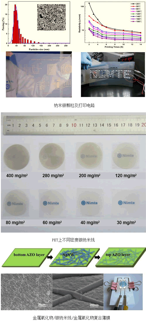
Printed electronics technology is the use of traditional printing technology to manufacture electronic devices and systems of science and technology. Compared with the traditional silicon-based microelectronics manufacturing technology, the electronic devices prepared by this technology have the characteristics of large area, flexibility, and low cost. As a flexible, rapid, and environmentally friendly manufacturing method, printed electronics technology has become a hot topic in the materials, electronics, and manufacturing industries. The Song Weijie team of the Ningbo Institute of Materials Technology and Engineering, Chinese Academy of Sciences used silver nanomaterials as research objects to controllably produce silver nanoparticle and silver nanowire printing inks, which were further developed using film-forming techniques such as printed electronics and blend spin coating. Various types of substrate conductive film. From the preparation of environment-friendly, colorless, transparent, and stable particle-free organic silver precursor inks, an electronic circuit with a resistivity of 3.1 μΩcm was prepared using an ink-jet printing technique, and a silver solar cell line was further prepared by ink-jet printing. . The method realizes the controllable preparation of the silver electronic circuit in terms of graphics and width and thickness, which can greatly increase the production efficiency, reduce the use of silver, and reduce the device cost. Related work Published papers and patents: Applied Surface Science, 2012, 258(19), 7384 and 102286226A (licensed). Silver nanoparticles are rapidly and massively prepared by a simple method. Silver particles are stored in solid state without deterioration. Silver-particle inks with stable performance are obtained by dispersing in an environmentally friendly aqueous solution. The stability mechanism of silver particles in the ink is studied, and ink jet printers are used. In the plastic, paper and other flexible substrates to prepare strong adhesion, high conductivity LED circuits, RFID tags, electromagnetic shielding materials, and discussed the feasibility of room temperature chemical sintering silver particles. Related work Published papers: Nanoscale, 2014, 6(3), 1622, Materials Chemistry and Physics, 2014, 147(3), 550, Materials Letters, 2014, 123, 124; Patent A (licensed), 102816462A (authorized ). Using mild and environmentally friendly synthesis methods, silver nanowires with good aspect ratio and uniformity of distribution were successfully prepared and can be placed in a solid state and dispersed when needed. Further, high-transmittance, low-resistance two-dimensional and three-dimensional transparent conductive films were prepared on the basis of polymers such as PET, PI, and cellulose, exhibiting excellent flex resistance. At the same time, this type of film can be used in the field of high-performance electric heating, achieving a good function of defogging and heating. The cellulose-based film is more environmentally friendly and biodegradable, and may be the next choice for direct contact with skin-like wearable devices. Relevant working papers will be published in materials letters and other journals. The silver nanowire film has excellent photoelectric properties and flexibility, but the pure silver nanowire film has a large surface roughness and poor adhesion to the substrate. The research group used magnetron sputtering, spin coating, and roll coating to fabricate metal oxide/silver nanowire/metal oxide sandwich composite films on flexible substrates of PET and PI, further increasing the resistance of the films. With the bending performance and weatherability, the composite film is expected to be applied in the fields of flexible electronic devices, energy storage and photovoltaic devices. Related work Published paper: Journal of Materials Chemistry C, 2014, 2(19), 3750, ACS applied materials & interfaces, 2015, 7(7): 4299; Patent A, 103730194A. The above work was supported by projects of the National Natural Science Foundation of China, Natural Science Foundation of Zhejiang Province, and Natural Science Foundation of Ningbo City.
Copper chrome interior wall faucet, also called Copper chrome Pipe embedded faucet, in Putie tiles before to pipeline embedded into the wall, leaving the mouth and rain water outlet temperature in advance and export, depends on the specific buying styles depending on the installation technology requirements are relatively high. The advantages of copper chrome plated Inner Wall Faucet are beautiful, concise and save space. Therefore, many family bathrooms will be installed Copper chrome Pipe embedded faucet, such sanitary products, high-end hotels will also be installed. After all, the copper chrome plated interior wall faucet can greatly improve the quality of the hotel, but also save room space.
Inner wall faucet​ Inner Wall Faucet,​Handheld Bathroom Faucet,Inner Wall Shower Faucet,Copper Inner Wall Faucet KaiPing Dongsheng Sanitary Ware Industrial Co.,Ltd. , https://www.dsfaucet.com